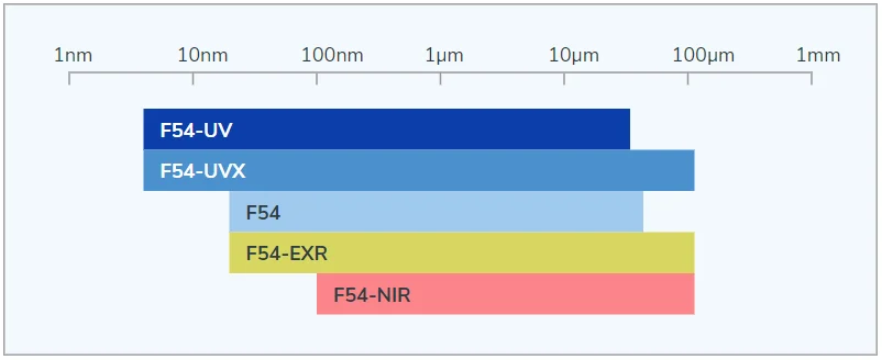
Product Description
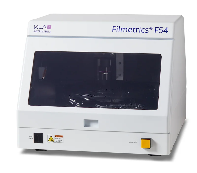
Thin-film thickness of samples up to 450mm in diameter are mapped quickly and easily with the F54 advanced spectral reflectance system. The motorized R-Theta stage moves automatically to selected measurement points and provides thickness measurements as fast as two points per second. Autofocus and microscopic spot size are standard features on this advanced spectral reflectance tool.
The F54 can be connected to the user laptop in minutes and be used to provide thickness measurement as fast as two points per second. The system includes dozens of predefined polar, rectangular, or linear map patterns, with the added ability for the user to create their own map pattern with unlimited measurement points.
Product Features
- Microscopic spot size
- Built-in integrated video camera
- Auto-focus (motorized Z-stage)
- Intuitive analysis software standard with every system
- 24-hour (M-F) phone, email, and online support from highly trained application engineers
- System package includes integrated spectrometer/light source unit, microscope adapter, reflectance standards, thickness standards and more!
Applications
Automated thin-film thickness mapping of most smooth, non-metallic film layers including:
- SiO2
- Photoresist
- SiNx
- Polymer layers
- DLC
- Polyimide
- Polysilicon
- Amorphous Silicon
Industries
Semiconductor Fabrication
- Photoresist, Oxides/nitrides/SOI, Wafer backgrinding
LCDs
- Cell gaps, polyimide, ITO and other TCOs
Optical Coatings
- Hardcoat thickness, Anti-reflection coating, Filters
MEMS
- Photoresist
- Silicon membranes
- AlN/ZnO Thin-Film Filter
Look at the Industries tab for additional details.